System BLUE
2041 words Estimated reading time 8 minutes
The Lightning Detector System Blue is a universal receiver for electromagnetic waves in the VLF/LF frequency range between 3 kHz and 300 kHz. It has three input channels for H-field antennas and one input channel for an E-Field antenna. The following two criteria played a crucial rule during the design of the detector.
- The detector should not be too expensive for the end user.
- The detector should provide the user with a variety of experimental possibilities.
The Kit
The main difference between System Blue and previous systems is that System Blue has partly prefabricated circuit boards. All surface-mount devices (SMD) are already soldered. However, there are still some components with leads that have to be inserted into holes drilled in the printed circuit boards and soldered to pads on the back side by manual assembly. For soldering you should use a soldering iron with a 1mm tip and thin solder wire. Do not try to solder these components if you do not have any experience with soldering electronic parts.
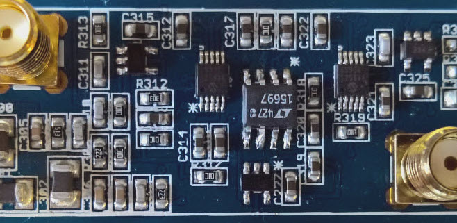
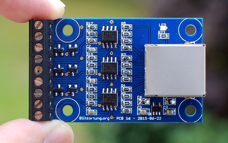
The board with the identification PCB 20.x is a panel consisting of a main board PCB 19.x an H-field preamplifier PCB 16.x and an E-field preamplifier PCB 17.x. The latest version of September 2017 is the panel PCB 20.5 with the main board 19.4 the H-field preamplifier PCB 16.1 and the E-field preamplifier PCB 17.1.
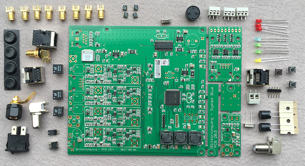
The following picture shows a complete set with all parts. Not all of these parts are essential for the operation of the detector. The 8 SMA jacks are not supplied. The maximal 4 filter ICs can be purchased separately and are not included as standard. The 3mm light-emitting diodes, the switch, the rubber feet and the grounding socket are only necessary if the main board is installed in the housing. These parts are only included if the housing is ordered.
Assembly
In the following chapters youe will find detailed assembly instructions. Some of our members also recorded the assembly of their stations on video.
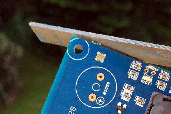
Separate the boards
You can separate the boards manually. After that, you should file off the overhanging edges.
Controller board PCB 19.x
The controller board PCB 19.x has the following through-hole technology (THT) components.
- 3 x DA103C - Transformer - Murata Power Solutions
- 1 x Inductor - 3.3 mH - Taiyo Yuden
- 1 x USB Mini-B Connector, PCB mounting, 90°
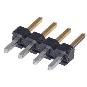
- 1 x 1x4 Header, straight, Pitch 2,54 (only 19.1/19.2/19.3)
- 1 x 1x5 Header, straight, Pitch 2,54 (only 19.1/19.2/19.3)
- 1 x 2x5 Header, straight, Pitch 2,54 (only 19.4)
- 1 x 1x2 Header, straight, Pitch 2,54 (only 19.4)
- 1 x 2x3 Header, straight, Pitch 2,54 (only 91.1/19.2/19.3)
- 1 x Jumper (only 91.4)
- 2 x Jumpers (only 91.1/19.2/19.3)
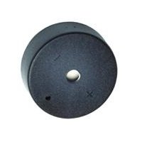
- 1x Piezo Audio Indicator
- 1x Crystal, 8.0000000 MHz
- 1x Crystal, 25.000000 MHz
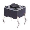
- 3 x Pushbutton 6x6mm, height: 4,3mm, vertical
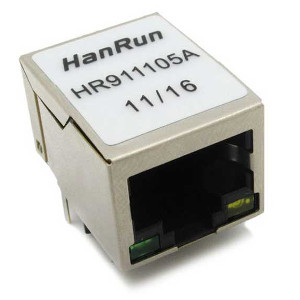
- 1 x RJ45 Modular Connector
- 1 x HanRun (HR911105A) RJ45 network connector with integrated magnetics
- 1 x F-Connector, PCB mounting, 90°
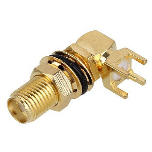
- 1 x SMA Connector, PCB mounting, 90°
- 1 x Ground Socket (only PCB 19.4)
Some of the THT components may have been soldered because they were required to install the initial firmware.
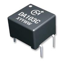
The DA103C Transformers have a white dot at one corner. On the main board, there are white dots printed at the placeholders for the transformers TR1, TR2, and TR3. The white dots at the transformers must match the white dots at the main board.
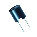
The 3.3mH inductor is L403.

Crystal Q1 has a frequency of 25 MHz, crystal Q2 has a frequency of 8 MHz.
Some Piezo Audio Indicators have a ’+’-mark, which should match the ’+’-mark on the board. (If there is no ’+’-mark, then the orientation is not important.)


All other components can not be soldered at wrong places because of their physical layout.
Power supply
Note
Please use a 1 Ampere or bigger power supply. We have had some bad experiences with 500mA power supplies.
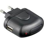
The main board is supplied with a 5V USB power adapter. The plug must be a USB-B Mini 5 pin. The power supply is not part of the kit and must be purchased separately. The power consumption is about 450mA.

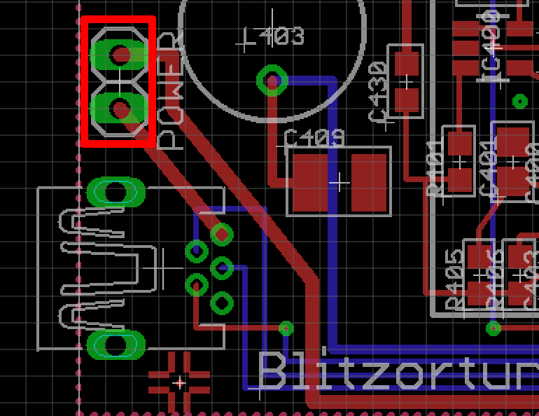
At switch S1 on PCB 19.2 you have to connect pin 5 and pin 6 with a jumper. This turns the board on, if a USB power supply is connected, shown by the red rectangle in the image below. You must connect pin 1 and pin 2 a jumper so that the pre-amplifiers get power, shown by the green rectangle in the image below. Note that these jumper settings are different from the early board PCB 19.1. Please refer to the circuit diagrams. At 19.4 you must connect the two pins of the power jumper.
Network connection
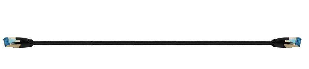
The router is connected at the RJ45 network port with a shielded twisted pair network cable (FTP, STP, S/STP, or S/FTP). More information about accessing the web interface can be found here.
Digital filter option
The complete digital filter option consists of
- 4 x digital filter ICs (LTC1569-7)
- 8 x SMA Connector, PCB mounting
In general, it is not necessary to install the digital filter ICs. The system also operates without them. However, if you want to experiment, or if you have extremely strong interference at frequencies above 20kHz, you can try to get better signals with the digital low pass filter ICs. Since the digital filter ICs are relatively expensive, you should test one filter IC at one channel, preferably at the E-Field channel. If the desired effect is achieved, the other channels can be upgraded.
The digital filter ICs have a point at one corner of the housing. This point identifies Pin 1. It must match the white dot on the main board. You need a soldering iron with a small tip to solder the SOIC-8 package.
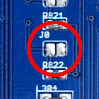
You have to close (solder) Jumper J0, otherwise the firmware will not recognize the filter ICs, and thus will not allow you to adjust them.
All inputs and outputs of the amplifiers are passed via buffer amplifiers to SMA connectors. If these connectors are installed, then the signals can easily be monitored with an oscilloscope or an FFT analyzer. There are various computer programs for signal analysis, if the output of the preamplifier is passed in to the PC via a sound card.
Housing option
The housing option consists of the following parts.
- 1 x aluminum enclosure
- 1 x front panel
- 1 x back panel
- 1 x rocker switch
- 8 x screw M3 10mm
- 4 x rubber feet
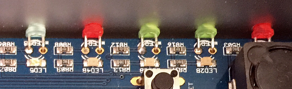
- 3 x LED red
- 2 x LED green
- 1 x LED yellow
- 1 x LED blue

The housing is made for boards of size 130.0 mm x 140.0 mm. The main board PCB 19 has the dimension 130.0 mm x 138.5 mm and is slightly shorter than the housing. The LEDs on the front panel are soldered with an angle of 90 degrees. The overlapping edge of the LED housing closes the gap between the board and the front panel. In this construction, the LED can not be crushed by pressure from outside at the front panel, which is the reason for the difference in size between the housing and the main board.

The threads at the corners in the aluminum housing are drilled by machine. Any protruding metal chips must be removed with a screwdriver or a wooden stick otherwise they may be fall onto the board. Do not use your finger to clean the threads.

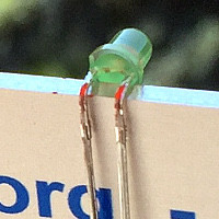
The connecting wires of the LEDs can easily be bent 90 degrees using the front panel that has a width of 2 mm. On the main board there are white stars printed near the LEDs. In these holes the short ends of the wires have to be inserted. This is the cathode (-) of the diodes.
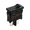
At the back panel, the rocker switch can be inserted to turn the power on and off. It has to be connected to pin 5 and 6 of S1 (19.1/19.2/19.3) or at the power jumper (19.4).

The rubber feet can be stuck under the housing.
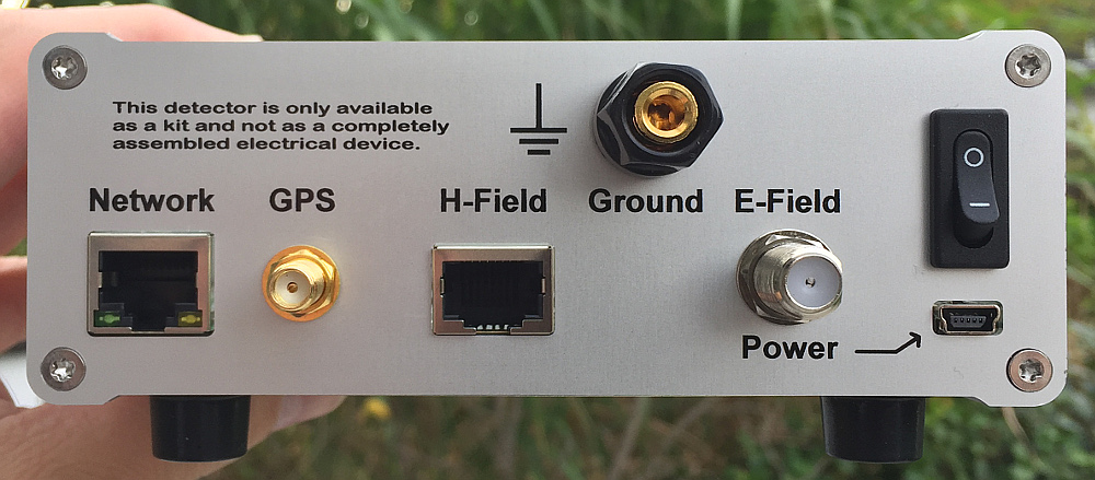

From version 19.4 a pole terminal for connecting ground is included. The layout of the back panel has also changed. The ethernet controller was placed a little further away from the amplifiers. The Ethernet socket has been swapped with the GPS socket.
Voltage regulator extension (PCB 19.1/19.2 only)
Unfortunately, the voltage regulators of the boards PCB 19.1 and PCB 19.2 are not adequate for the current consumption of the boards. This problem is eliminated by the piggyback board PCB 21.

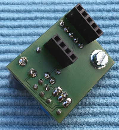
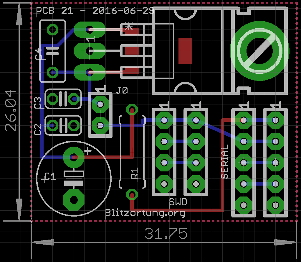
PCB 21 is manufactured on a panel with severals boards and thus may have overhanging edges. You should file off these edges.
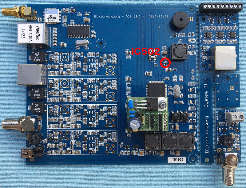
The voltage regulator IC502 should be unsoldered from the board. Please do not operate with both voltage regulators. They can act against each other.
H-field pre-amplifier PCB 16.x
The H-field pre-amplifier board PCB 16.x has the following THT components whose placement is obvious.
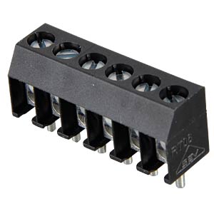
- 1 x Header 3-pin, Pitch 3.5mm
- 1 x Header 6-pin, Pitch 3.5mm (or alternatively 2 x Header 3-pin, Pitch 3.5mm)
- 1 x RJ45 Modular Connector

| 1 | 2 | 3 | 4 | 5 | 6 | 7 | 8 | 9 |
|---|---|---|---|---|---|---|---|---|
| A-1 | A-2 | GND | B-1 | B-2 | GND | C-1 | C-2 | GND |

The antennas are connected to the pre-amplifier as shown above. The screw strip is intended for connecting the wires of loop antennas. The wires of ferrite rod antennas have to be soldered to the back of the board. They cannot be screwed. These wires are insulated with varnish. Before these wires are soldered, the varnish must be scraped off with a knife.
The H-field pre-amplifier is connected with a shielded twisted pair cable (FTP, STP, S/STP, or S/FTP) to the main board. This cable should not be placed next to the network cable. Please keep a distance of at least 10 cm. The cable may have a length of up to 30 meters.

If you use loop antennas, than you should close (solder) the jumper for the corresponding channels at the back side of the board.
If the pre-amplifier is powered, the red LED should light.
E-field pre-amplifier PCB 17.x
The E-field pre-amplifier board PCB 17.x has the following THT components whose placement is obvious.
- 1 x Inductor - 3.3 mH - Taiyo Yuden
- 1 x Header 2-pin, Pitch 5.08mm
- 1 x F-Connector, PCB mounting
In panel PCB 20.1 and subsequent panels the free board space next to PCB 17.x is used as an experimental electrical antenna. This antenna is designed only for testing purposes. Due to a small manufacturer's error on Panel 20.5, the printed circuit board next to the E-field preamplifier is not connected to the input of the E-field preamplifier. Here, either a small solder bridge must be made or a corresponding antenna must be connected to the input. You can also break off this aerial and connect a wire antenna at the two pin header. The external connection point is ground, the central connection point is the antenna. Note that any electrical antenna must be placed outside far away from buildings and electrical interference sources.
The E-field pre-amplifier is connected with 75 Ω double shielded coaxial cable to the main board. The cable may have a length of up to 100 meters. The ends are attached to F-connector.
When the pre-amplifier is powered, the red LED should light. On the early pre-amplifier board 16.1 the green LED probably lights very weakly with a supply voltage of 3.3 volts. However, this is not a defect and is normal.